Slika:Opamptransistorlevelcolored.png
Transistor-level schematic for a 741 op-amp, color coded.
Povzetek
(See w: Op-amp#Internal_circuitry_of_741_type_op-amp for the most recent description.)
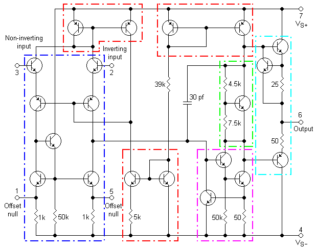
From the diagram, the blue section is a differential amplifier. The base current of the inputs is not really zero, giving the 741 an input impedance of about 2 MΩ.
The sections in red are current mirrors. The input amplifier drives a current mirror load. The top left current mirror allows large common-mode voltages on the inputs without exceeding the active range of any transistor in the circuit. The top right current mirror provides a constant current load for the output circuitry, regardless of the output voltage . The lower current mirror has a very low collector current, because of the 5 kΩ resistor. It is used as a high-impedance connection to the negative power supply, to provide a reference without loading the input circuitry.
The offset null pins are used to remove any offset voltage that would exist at the output of the op-amp when zero signal is applied to the inputs.
The high voltage gain stage is NPN.
The green section is a voltage level shifter. It provides a constant voltage drop between the top and the bottom regardless of supply voltage. If the base current to the transistor is zero, and the voltage between base and emitter (and across the 7.5 kΩ resistor) is 0.625 V (a typical value for a BJT), then the current flowing through the 4.5 kΩ resistor will be the same, and will produce a voltage of 0.375 V. This keeps the voltage across the transistor, and the two resistors at 0.625 + 0.375 = 1 V. This serves as a bias for the two output transistors, to prevent crossover distortion. In some amps this function is achieved with diodes.
The capacitor is used as part of a low pass filter (on the base of an emitter follower) to reduce the frequency response of the amp to prevent oscillations. This technique is called Miller Compensation and functions as an internal capacitive feedback.
The output in cyan is a push-pull emitter follower amplifier. It is driven by a PNP emitter-follower. The output range of the amplifier is about 1 volt less than the supply voltage, since the collector-emitter voltage of the output transistors can never go completely to zero. The resistors in the output mean that the current provided by the output is limited (about 25 mA for the 741), and the output resistance is not zero without feedback. With negative feedback it approaches zero. The output stage has current limiting circuitry.
- Opis wyprowadzeń (cyfry oznaczają numery wyprowadzeń w standardowej obudowie ośmiokońcówkowej, końcówka nr 8 - nieużywana)
- Offset null - balans zera
- Inverting input - wejście odwracające
- Non-inverting input - wejście nieodwracające
- Vs- - minus zasilania
- Offset null - balans zera
- Output - wyjście
- Vs+ - plus zasilania
Op-amp transistor level
-
 Transistor level diagram of an op-amp
 -
 Sectioned transistor level diagram of an op-amp
 -
 Sectioned transistor level diagram of an op-amp with labeled transistors


Created by User:Omegatron using Klunky schematic editor, which the creator considers public domain (possibly with post-editing in the GIMP or Inkscape)
- Dovoljeno vam je:
- deljenje – reproducirati, distribuirati in javno priobčevati delo
- predelava – predelati delo
- Pod naslednjimi pogoji:
- priznanje avtorstva – Navesti morate ustrezno avtorstvo, povezavo do licence in morebitne spremembe. To lahko storite na kakršen koli primeren način, vendar ne na način, ki bi nakazoval, da dajalec licence podpira vas ali vašo uporabo dela.
- deljenje pod enakimi pogoji – Če boste to vsebino predelali, preoblikovali ali uporabili kot izhodišče za drugo delo, morate svoj prispevek distribuirati pod isto ali združljivo licenco, kot jo ima izvirnik.

|
Ta dokument je dovoljeno kopirati, razširjati in/ali spreminjati pod pogoji Licence GNU za prosto dokumentacijo, različica 1.2 ali katera koli poznejša, ki jo je objavila ustanova Free Software Foundation; brez nespremenljivih delov ter brez besedil na sprednji ali zadnji platnici. Kopija licence je vključena v razdelek Licenca GNU za prosto dokumentacijo. |
(In short, this means that you can copy and modify the image freely as long as you provide attribution; preferably in the form of a link back to this page.)

|
File:OpAmpTransistorLevel Colored.svg je vektorska različica te datoteke. Treba jo je uporabiti namesto te rastrske slike.
File:Opamptransistorlevelcolored.png → File:OpAmpTransistorLevel Colored.svg
Več informacij o vektorski grafiki je na voljo na strani Commons:Transition to SVG. Na voljo so tudi informacije o podprtosti SVG-slik v programju MediaWiki. |
 |
Zgodovina datoteke
Kliknite datum in čas za ogled datoteke, ki je bila takrat naložena.
| Datum in čas | Sličica | Velikost | Uporabnik | Komentar | |
|---|---|---|---|---|---|
| trenutno | 20:36, 26. junij 2005 | | 618 × 488 (10 KB) | wikimediacommons>Omegatron | An electrical diagram created by User:Omegatron. (Uploaded with Wikimedia Commonplace.) Source: Created by User:Omegatron {{GFDL}}{{cc-by-sa-2.0}} Category:Electrical diagrams\ |
Uporaba datoteke
Datoteko uporablja naslednja 1 stran: